Marantz PM7200 repair
During the last RepairCafe I got a Marantz PM7200 amplifier in my hands that had a very interesting fault.
Whenever the output signal reached a certain level, the amplifier switched the outputs off (as I learned later on, that is called the protection mode). This symptom could be provoked by either increasing the input level or increasing the amplification by turning the volume control. The effect occurred on the left and right channel. It didn’t matter if I put a signal at both or only at one channel. Also the source of the signal didn’t matter.
For “on the road” signal generation I use the android app called “Function Generator” (https://play.google.com/store/apps/details?id=com.keuwl.functiongenerator&hl=de).
My first guess was that the output stage must have a problem (shorted output transistor or something similar). However I measured no significant DC offset and all the signals seem to be just fine. My second guess was a thermal issue but that also led me to nothing significant. I also measured the power supply and all the other “most likely suspects” … nothing turned up. So sadly I wasn’t able to repair the amplifier at the RepairCafe and decided to take it with me to investigate further.
At home I did some more testing. The problem was also independent of the Mode (Class AB or Class A) and also seemed to be invariant of the frequency (I tested from 50 Hz to approximately 10 kHz). Another strange effect was that the error was instantly resettable. When the amplifier switched the outputs off you just had to reduce the volume a bit and it instantly turned back on again. The fast reaction seemed to make a thermal issue very unlikely.
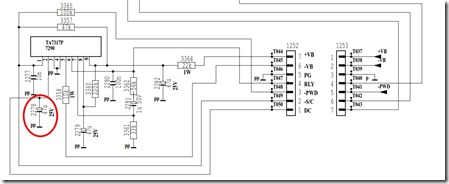
If you search on the internet, you can find a service manual which is really helpful because it has all the schematics in it. Because all the signals I measured so far seemed fine, I decided to investigate the protection circuit and measure the signals there. By studying the schematic of the main amplifier one can see, that at the end of the output stages the signal gets tapped of to the protection circuit (marked with the red box). This signal is for DC offset detection.
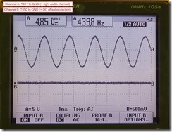
I fed a sine wave (440 Hz, 500 mVpp) to the right and left channel (0° phase shift). I increased the volume so that the error just show up. When I measured the signal (T050 to GND) I saw the same signal shape as at the output stage (T017 to GND). The measurement is shown at the screenshot below. The test points are marked green in the schematic above.
The protection circuit has a TA7317P IC in it. If you look at the datasheet you see that the IC will send the amplifier to protection mode when a voltage level of approximately 1 V is exceeded. With this information it seems plausible that (given the signal at T050 as shown above) the amplifier switches to protection mode.
My next test was to fed in the same signal as before (440 Hz, 500mVpp) but this time I shifted the phase of the left channel by 180°. My thought was, that with the phase shifted input signal, there should be no signal at T050 (left and right signal cancel each other out). With the so fed signal the amplifier didn’t show the error anymore! This led me to the conclusion that the amplifier is probably working fine and just the protection circuit has a defect.
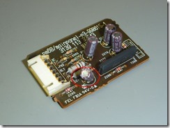
Some further investigation showed, that there is a capacitor (2278) attached to the DC offset line that should flatten all the AC signals. When I measured the capacitor with the LCR-Meter there was no reading of the capacitance possible (the capacitor was dead). I replaced the capacitor with a new one with the same values (I used a 105 °C rated) and did the first measurement (with 0° phase shift) once more.
As to be expected the signal at T050 changed drastically. All the AC part was gone and the amplifier didn’t turn off anymore! Yeah … problem found and fixed!
To be safe I replaced all four electrolytic capacitors (2278, 2281, 2282, 2279) on the protection board. I measured them later on and they all where in pretty bad condition.
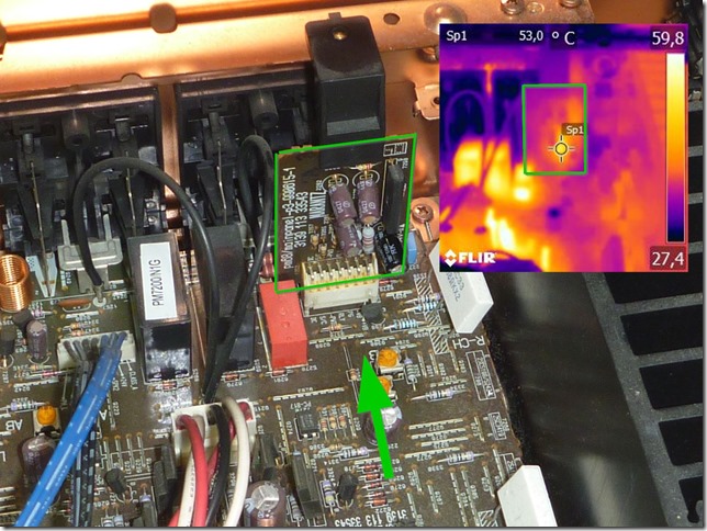
I did some thermal imaging of the protection circuit board. The picture above was taken after 5 minutes idle time of the amplifier (switched on but no signal). The green arrow indicates the approximate direction of the IR Image. The green frame marks the protection circuit board. As you can see there is a hotspot (53 °C) very close to the broken capacitor caused by two 1 W resistors (3364 and 3358). The permanent exposure to heat probably killed the capacitors.
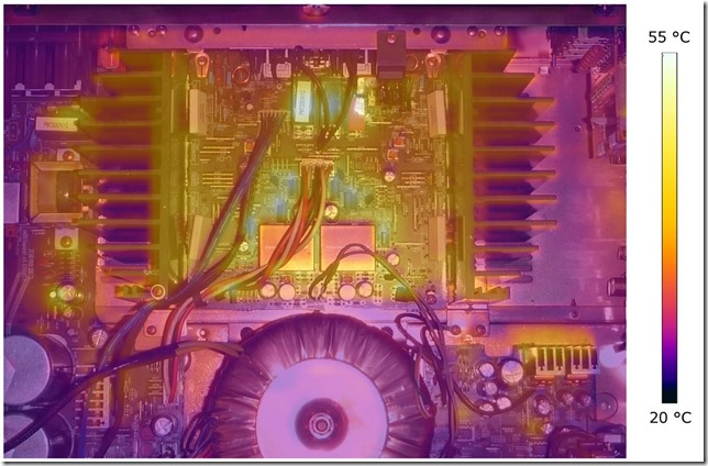
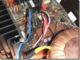
I also did a thermal image of the whole main amplifier board to find other hotspots. To recognize the components better, I made an overlay with a normal picture (I used gimp for that). The overlay is not perfect because of an slightly different angle and focal length of the two cameras. You can see that there are areas that get 55 °C hot if the amplifier is idle (the picture was taken after 10 minutes idle time). In the center area there are some linear regulators that have capacitors close by. I measured some of those capacitors and all seem to have degraded so I went ahead and replaced the ones that where close to heat sources (2264, 2263, 2256, 2255, 2268, 2267).
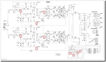
In the schematic above I marked all the components that I replaced. If you replace them, be sure to use 105 °C rated capacitors. The capacitors of the power supply where ok so I didn’t replace them. Be sure to do a DC offset voltage alignment and an idling current adjustment after you replace those components. At my unit the values have drifted a bit. You find detailed instructions on how to perform this adjustment in the service manual at page 34.
I tested the amplifier for several hours (at reasonable loud volume) and no error occurred. Fixed ![]()


